WO2021005967A1 - インダクタ - Google Patents
インダクタ Download PDFInfo
- Publication number
- WO2021005967A1 WO2021005967A1 PCT/JP2020/023262 JP2020023262W WO2021005967A1 WO 2021005967 A1 WO2021005967 A1 WO 2021005967A1 JP 2020023262 W JP2020023262 W JP 2020023262W WO 2021005967 A1 WO2021005967 A1 WO 2021005967A1
- Authority
- WO
- WIPO (PCT)
- Prior art keywords
- housing
- coil
- external electrode
- mounting surface
- inductor
- Prior art date
Links
- 239000004020 conductor Substances 0.000 claims abstract description 38
- 238000004804 winding Methods 0.000 claims abstract description 27
- 239000000758 substrate Substances 0.000 claims abstract description 20
- 239000011810 insulating material Substances 0.000 claims description 7
- 238000012986 modification Methods 0.000 description 4
- 230000004048 modification Effects 0.000 description 4
- 239000002904 solvent Substances 0.000 description 4
- RYGMFSIKBFXOCR-UHFFFAOYSA-N Copper Chemical compound [Cu] RYGMFSIKBFXOCR-UHFFFAOYSA-N 0.000 description 3
- 238000013459 approach Methods 0.000 description 3
- 239000000919 ceramic Substances 0.000 description 3
- 239000012212 insulator Substances 0.000 description 3
- 239000000463 material Substances 0.000 description 3
- 239000007769 metal material Substances 0.000 description 3
- 239000002923 metal particle Substances 0.000 description 3
- 239000002245 particle Substances 0.000 description 3
- PXHVJJICTQNCMI-UHFFFAOYSA-N Nickel Chemical compound [Ni] PXHVJJICTQNCMI-UHFFFAOYSA-N 0.000 description 2
- 239000011230 binding agent Substances 0.000 description 2
- 238000010030 laminating Methods 0.000 description 2
- 239000000696 magnetic material Substances 0.000 description 2
- 238000009751 slip forming Methods 0.000 description 2
- BQCADISMDOOEFD-UHFFFAOYSA-N Silver Chemical compound [Ag] BQCADISMDOOEFD-UHFFFAOYSA-N 0.000 description 1
- 229910010293 ceramic material Inorganic materials 0.000 description 1
- 229910052802 copper Inorganic materials 0.000 description 1
- 239000010949 copper Substances 0.000 description 1
- 238000005238 degreasing Methods 0.000 description 1
- 239000003989 dielectric material Substances 0.000 description 1
- 238000000605 extraction Methods 0.000 description 1
- 238000004519 manufacturing process Methods 0.000 description 1
- 238000000034 method Methods 0.000 description 1
- 229910052759 nickel Inorganic materials 0.000 description 1
- 230000002093 peripheral effect Effects 0.000 description 1
- 230000035699 permeability Effects 0.000 description 1
- 239000011347 resin Substances 0.000 description 1
- 229920005989 resin Polymers 0.000 description 1
- 229910052709 silver Inorganic materials 0.000 description 1
- 239000004332 silver Substances 0.000 description 1
Images


Classifications
-
- H—ELECTRICITY
- H01—ELECTRIC ELEMENTS
- H01F—MAGNETS; INDUCTANCES; TRANSFORMERS; SELECTION OF MATERIALS FOR THEIR MAGNETIC PROPERTIES
- H01F27/00—Details of transformers or inductances, in general
- H01F27/28—Coils; Windings; Conductive connections
- H01F27/29—Terminals; Tapping arrangements for signal inductances
- H01F27/292—Surface mounted devices
-
- H—ELECTRICITY
- H01—ELECTRIC ELEMENTS
- H01F—MAGNETS; INDUCTANCES; TRANSFORMERS; SELECTION OF MATERIALS FOR THEIR MAGNETIC PROPERTIES
- H01F17/00—Fixed inductances of the signal type
-
- H—ELECTRICITY
- H01—ELECTRIC ELEMENTS
- H01F—MAGNETS; INDUCTANCES; TRANSFORMERS; SELECTION OF MATERIALS FOR THEIR MAGNETIC PROPERTIES
- H01F27/00—Details of transformers or inductances, in general
- H01F27/02—Casings
-
- H—ELECTRICITY
- H01—ELECTRIC ELEMENTS
- H01F—MAGNETS; INDUCTANCES; TRANSFORMERS; SELECTION OF MATERIALS FOR THEIR MAGNETIC PROPERTIES
- H01F27/00—Details of transformers or inductances, in general
- H01F27/28—Coils; Windings; Conductive connections
- H01F27/2823—Wires
-
- H—ELECTRICITY
- H01—ELECTRIC ELEMENTS
- H01F—MAGNETS; INDUCTANCES; TRANSFORMERS; SELECTION OF MATERIALS FOR THEIR MAGNETIC PROPERTIES
- H01F5/00—Coils
- H01F2005/006—Coils with conical spiral form
Definitions
- the present disclosure relates to an inductor having a conical coil.
- Patent Document 1 discloses a chip-type inductor in which a winding is wound around a core.
- a winding is wound around a dogbone type core having different diameters at the start and end of winding of the coil, and a resistant conductor is installed flat on the top surface.
- Patent Document 2 discloses an inductor in which the exterior of the housing is omitted and a winding is wound around the core.
- the inductor disclosed in Patent Document 2 has a structure in which the lead electrode (lead) from the coil is shortened or eliminated, so that the stray inductance value is lowered. In this case, since the extraction electrode is short, this coil is attached to the mounting substrate by inclining the winding shaft of the coil.
- JP-A-2017-108058 Japanese Unexamined Patent Publication No. 2009-231518
- the inductor described in Patent Document 2 does not have a lead for external drawing from the coil, so that if the chip is made smaller, the pick-up property at the time of mounting is poor. Further, an electrode for connecting to the substrate is provided at the tip of the small diameter portion of the coil. However, as the coil tip diameter becomes smaller, the external electrode also becomes smaller, which causes a problem that the solderability deteriorates.
- An object of an embodiment of the present invention is to provide an inductor that can suppress stray inductance and can be miniaturized.
- One embodiment of the present invention is an inductor, which is a rectangular body formed of an insulating material, a conical coil embedded inside the housing, and a substrate mounting surface of the housing.
- the conical coil includes a first external electrode provided at an end portion and a second external electrode provided at the second end portion of the substrate mounting surface of the housing, and the conical coil is spirally wound. It is formed by a coil conductor embedded in the housing, the winding axis direction of the conical coil is inclined with respect to the substrate mounting surface of the housing, and both ends of the coil conductor are of the housing.
- the first external electrodes and the second external electrodes located at both ends of the board mounting surface of the housing are connected so that the board mounting surface side is an end portion.
- the stray inductance can be suppressed and the inductor can be miniaturized.
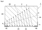
- FIG. 3 It is a perspective view which shows the inductor according to the embodiment of this invention. It is a top view which shows the inductor in FIG. It is sectional drawing which saw the inductor in the direction of arrow III-III in FIG. It is a top view which shows the inductor by the 1st modification. It is sectional drawing at the same position as FIG. 3 which shows the inductor by the 2nd modification.
- the inductor 1 includes a housing 2, a conical coil 3, a first external electrode 5, and a second external electrode 6.
- the housing 2 (package) is formed of an insulating material such as a ceramic material.
- the insulating material of the housing 2 may be a magnetic material or a non-magnetic material.
- the insulating material of the housing 2 may be a dielectric material or a resin material.
- the housing 2 is formed in a rectangular parallelepiped shape, for example.
- the housing 2 has a first main surface 2A (first end surface) and a second main surface 2B (second end surface) facing each other.
- the housing 2 has a board mounting surface 2C as a bottom surface and a top surface 2D facing the board mounting surface 2C.
- the first main surface 2A and the second main surface 2B are located at the first end portion and the second end portion in the length direction (left-right direction in FIG. 3) of the board mounting surface 2C.
- the conical coil 3 is formed by a coil conductor 4 that is spirally wound and embedded in an insulator of a housing 2. Therefore, the conical coil 3 is provided inside the housing 2.
- the conical coil 3 is formed by a coil conductor 4 wound in a spiral shape.
- the coil conductor 4 is formed of a conductive metal material such as copper, nickel, silver, etc. as the conductive material.
- the coil conductor 4 is formed in an elongated strip shape.
- the coil conductor 4 includes a coil portion 4A wound in a conical shape, an electrode connecting portion 4B connected to the first end portion of the coil portion 4A, and an electrode connecting portion connected to the second end portion of the coil portion 4A. It is equipped with 4C. Both ends of the coil conductor 4 are the first external electrodes 5 and the first external electrodes 5 located at both ends of the board mounting surface 2C of the housing 2 so that the board mounting surface 2C side (board side) of the housing 2 is the end. 2 It is electrically connected to the external electrode 6. At this time, the first end portion of the coil conductor 4 is located on the maximum diameter side of the conical coil 3 and is the large diameter side end portion of the conical coil 3. The first end portion of the coil conductor 4 is an electrode connecting portion 4B.
- the electrode connection portion 4B is arranged at a position close to the substrate mounting surface 2C of the housing 2 and close to the first main surface 2A of the housing 2.
- the second end portion of the coil conductor 4 is located on the minimum diameter side of the conical coil 3 and is the small diameter side end portion of the conical coil 3.
- the second end portion of the coil conductor 4 is an electrode connecting portion 4C.
- the electrode connection portion 4C is arranged at a position close to the substrate mounting surface 2C of the housing 2 and close to the second main surface 2B of the housing 2.
- the winding axis direction (winding axis O) of the conical coil 3 is inclined with respect to the board mounting surface 2C of the housing 2.
- the conical coil 3 has a conical shape.
- the conical coil 3 is arranged so that the outer peripheral surface of the conical coil 3 is along the substrate mounting surface 2C.
- the winding shaft O (central shaft) of the conical coil 3 penetrates a surface perpendicular to the board mounting surface 2C.
- the winding shaft O of the conical coil 3 is arranged at a position away from the substrate mounting surface 2C on the first main surface 2A side where the outer diameter of the conical coil 3 is large. Specifically, the portion of the winding shaft O on the maximum diameter side of the conical coil 3 is separated from the board mounting surface 2C by a distance equivalent to the radial dimension on the maximum diameter side of the conical coil 3.
- the winding shaft O of the conical coil 3 is arranged at a position close to the board mounting surface 2C on the second main surface 2B side where the outer diameter dimension of the conical coil 3 is small. That is, the winding shaft O is closer to the board mounting surface 2C on the minimum diameter side of the conical coil 3 than on the maximum diameter side of the conical coil 3. In this way, the winding shaft O of the conical coil 3 approaches the board mounting surface 2C as it approaches the first main surface 2A to the second main surface 2B.
- the cross section of the coil conductor 4 has a rectangular shape.
- the long side of the cross section of the coil conductor 4 is parallel to the first main surface 2A and the second main surface 2B.
- the position accuracy of the conical coil 3 becomes high.
- the winding diameter of the conical coil 3 continuously increases as it approaches the first main surface 2A from the second main surface 2B.
- the insulating material of the housing 2 is arranged around the coil conductor 4 without a gap.
- the first external electrode 5 is provided in the housing 2.
- the first external electrode 5 is connected to the first end portion (electrode connecting portion 4B) of the coil conductor 4.
- the first external electrode 5 is formed of, for example, a conductive metal material as the conductive material.
- the first external electrode 5 is formed by being bent in an L shape from the first main surface 2A of the housing 2 to the substrate mounting surface 2C.
- the electrode connecting portion 4B of the coil conductor 4 is arranged close to the first external electrode 5. That is, the electrode connecting portion 4B is continuously formed at the first end portion of the coil portion 4A. Therefore, the length dimension from the coil portion 4A to the electrode connecting portion 4B is shorter than that in the case where the electrode connecting portion 4B and the first external electrode 5 are arranged apart from each other.
- the second external electrode 6 is provided in the housing 2.
- the second external electrode 6 is connected to the second end portion (electrode connecting portion 4C) of the coil conductor 4.
- the second external electrode 6 is formed of, for example, a conductive metal material as the conductive material.
- the second external electrode 6 is formed by being bent in an L shape from the second main surface 2B of the housing 2 to the substrate mounting surface 2C.
- the first external electrode 5 and the second external electrode 6 are arranged apart from each other.
- the electrode connecting portion 4C of the coil conductor 4 is arranged close to the second external electrode 6. That is, the electrode connecting portion 4C is continuously formed at the second end portion of the coil portion 4A. Therefore, the length dimension from the coil portion 4A to the electrode connecting portion 4C is shorter than that in the case where the electrode connecting portion 4C and the second external electrode 6 are arranged apart from each other.
- the inductor 1 according to the embodiment of the present invention has the above configuration.
- the inductor 1 is manufactured by a manufacturing method including the following three steps.
- an insulator ink composed of ceramic particles, an organic binder and a solvent, and a conductor ink composed of metal particles, an organic binder and a solvent are ejected by an inkjet method, and the solvent in each ink is repeatedly volatilized and dried.
- layers made of ceramic particles and metal particles are laminated one by one along the length direction of the housing 2 (left-right direction in FIG. 2).
- Each layer is formed, for example, parallel to the first main surface 2A and the second main surface 2B.
- a molded product composed of ceramic particles, metal particles, and an organic component is formed.
- the molded body does not need to be laminated in the length direction of the housing 2, and may be laminated in the height direction of the housing 2.
- the organic component of the molded product formed in the first step is removed.
- the third step the molded product from which the organic component has been removed in the second step is heated, and the insulator and the conductor are sintered at the same time. As a result, the housing 2 in which the conical coil 3 is built is formed.
- the first external electrode 5 and the second external electrode 6 are attached to the housing 2.
- the inductor 1 is completed.
- the first external electrode 5 is located on the first main surface 2A side of the housing 2, and is electrically connected to the first end portion (electrode connecting portion 4B) of the conical coil 3.
- the first external electrode 5 is located on the second main surface 2B side of the housing 2, and is electrically connected to the second end portion (electrode connecting portion 4C) of the conical coil 3.
- both ends of the coil conductor 4 are located at both ends of the board mounting surface 2C of the housing 2 so that the board mounting surface 2C side of the housing 2 is the end. It is connected to the external electrode 5 and the second external electrode 6.
- the line from the winding portion of the coil conductor 4 to the first external electrode 5 or the second external electrode 6 becomes shorter than that of the inductor disclosed in Patent Document 1. Therefore, the stray inductance becomes small.
- the shapes of the first external electrode 5 and the second external electrode 6 can be made the same on the left and right. Therefore, the inductor 1 can be easily mounted as compared with the inductor disclosed in Patent Document 2. In addition to this, since the housing 2 has a rectangular parallelepiped shape, it can be easily picked up by an automatic mounting machine.
- the inductor 1 is formed by sequentially laminating the inductor 1 without winding the winding around the core. Therefore, the radial dimension of the conical coil 3 can be reduced, and the inductor 1 can be miniaturized.
- the conical coil 3 is arranged at an oblique angle in the rectangular parallelepiped housing 2. Therefore, the maximum diameter of the conical coil 3 can be made larger than the height dimension of the housing 2. As a result, the inductance value can be obtained over a wide band from the high frequency band corresponding to the small diameter portion of the conical coil 3 to the low frequency band corresponding to the large diameter portion.
- the cross section of the coil conductor 4 is formed in a rectangular shape.
- the present invention is not limited to this, and the cross section of the coil conductor 4 may be a square shape, a circular shape, or an elliptical shape.
- a mark 12 for identifying the polarity of the conical coil 3 may be formed on the top surface 2D of the housing 2.
- the polarity identifier is not limited to the mark 12.
- half of the top surface 2D in the length direction of the housing 2 may be painted in a different color from the remaining portion to serve as a polarity identifier.
- the first external electrode 5 is formed from the first main surface 2A to the board mounting surface 2C
- the second external electrode 6 is formed from the second main surface 2B to the board mounting surface. It is formed over 2C.
- the present invention is not limited to this, and the first external electrode 22 and the second external electrode 23 may be formed on the substrate mounting surface 2C as in the inductor 21 according to the second modification shown in FIG. In this case, the first external electrode 22 does not have a portion facing the first main surface 2A. Similarly, the second external electrode 23 does not have a portion facing the second main surface 2B.
- the housing 2 is formed of a homogeneous material throughout.
- the present invention is not limited to this, and the inside of the housing may be filled with a material having a magnetic permeability larger than that of other portions, for example, located in the radial inner portion of the conical coil 3 to form a core. ..
- the inductor included in the above embodiment for example, the inductor described below can be considered.
- the first aspect is an inductor, which is a rectangular housing formed of an insulating material, a conical coil embedded inside the housing, and a first end of a substrate mounting surface of the housing.
- the conical coil is spirally wound to include a first external electrode provided in the portion and a second external electrode provided at the second end portion of the substrate mounting surface of the housing. It is formed by a coil conductor embedded in a housing, the winding axis direction of the conical coil is inclined with respect to the substrate mounting surface of the housing, and both ends of the coil conductor are the housing.
- the first external electrode and the second external electrode located at both ends of the board mounting surface of the housing are connected so that the board mounting surface side of the housing becomes an end portion.
- both ends of the coil conductor are connected to the first external electrode and the second external electrode located at both ends of the board mounting surface of the housing so that the ends are on the board mounting surface side of the housing. There is. As a result, the line from the winding portion of the coil conductor to the first external electrode or the second external electrode is short, so that the stray inductance becomes small.
- the shapes of the first external electrode and the second external electrode can be made the same on the left and right, it becomes easy to mount the inductor.
- the rectangular parallelepiped shape of the housing facilitates pick-up by an automatic mounting machine.
- the inductor has a conical coil embedded in the housing without winding the winding around the core. Therefore, the radial dimension of the conical coil can be reduced, and the inductor can be miniaturized.
- the conical coil is diagonally arranged in the rectangular parallelepiped housing. Therefore, the maximum diameter of the conical coil can be made larger than the height dimension of the housing. As a result, the inductor can obtain an inductance value over a wide band.
Landscapes
- Engineering & Computer Science (AREA)
- Power Engineering (AREA)
- Microelectronics & Electronic Packaging (AREA)
- Coils Or Transformers For Communication (AREA)
Priority Applications (3)
| Application Number | Priority Date | Filing Date | Title |
|---|---|---|---|
| CN202080047942.9A CN114072886A (zh) | 2019-07-11 | 2020-06-12 | 电感器 |
| JP2021530548A JPWO2021005967A1 (en]) | 2019-07-11 | 2020-06-12 | |
| US17/545,946 US20220102064A1 (en) | 2019-07-11 | 2021-12-08 | Inductor |
Applications Claiming Priority (2)
| Application Number | Priority Date | Filing Date | Title |
|---|---|---|---|
| JP2019129153 | 2019-07-11 | ||
| JP2019-129153 | 2019-07-11 |
Related Child Applications (1)
| Application Number | Title | Priority Date | Filing Date |
|---|---|---|---|
| US17/545,946 Continuation US20220102064A1 (en) | 2019-07-11 | 2021-12-08 | Inductor |
Publications (1)
| Publication Number | Publication Date |
|---|---|
| WO2021005967A1 true WO2021005967A1 (ja) | 2021-01-14 |
Family
ID=74114102
Family Applications (1)
| Application Number | Title | Priority Date | Filing Date |
|---|---|---|---|
| PCT/JP2020/023262 WO2021005967A1 (ja) | 2019-07-11 | 2020-06-12 | インダクタ |
Country Status (4)
| Country | Link |
|---|---|
| US (1) | US20220102064A1 (en]) |
| JP (1) | JPWO2021005967A1 (en]) |
| CN (1) | CN114072886A (en]) |
| WO (1) | WO2021005967A1 (en]) |
Citations (3)
| Publication number | Priority date | Publication date | Assignee | Title |
|---|---|---|---|---|
| JPH02235304A (ja) * | 1989-03-08 | 1990-09-18 | Matsushita Electric Ind Co Ltd | インダクタンス素子およびその製造方法 |
| JPH0367403U (en]) * | 1989-11-01 | 1991-07-01 | ||
| JPH0492607U (en]) * | 1990-12-27 | 1992-08-12 |
Family Cites Families (10)
| Publication number | Priority date | Publication date | Assignee | Title |
|---|---|---|---|---|
| TW362222B (en) * | 1995-11-27 | 1999-06-21 | Matsushita Electric Ind Co Ltd | Coiled component and its production method |
| JP3754406B2 (ja) * | 2002-09-13 | 2006-03-15 | 富士通株式会社 | 可変インダクタおよびそのインダクタンス調整方法 |
| KR100869741B1 (ko) * | 2006-12-29 | 2008-11-21 | 동부일렉트로닉스 주식회사 | 나선형 인덕터 |
| JP5084459B2 (ja) * | 2007-11-15 | 2012-11-28 | 太陽誘電株式会社 | インダクタ及びその製造方法 |
| JP2009290076A (ja) * | 2008-05-30 | 2009-12-10 | Shindengen Electric Mfg Co Ltd | 表面実装型インダクタの製造方法 |
| JP5603788B2 (ja) * | 2011-01-21 | 2014-10-08 | アンリツ株式会社 | コイルおよびその製造方法 |
| JP5821535B2 (ja) * | 2011-11-01 | 2015-11-24 | Tdk株式会社 | 積層型インダクタ |
| CN103050224A (zh) * | 2012-12-26 | 2013-04-17 | 王向群 | 功率电感器及其制造方法 |
| JP6695136B2 (ja) * | 2015-12-11 | 2020-05-20 | 株式会社村田製作所 | 巻線型インダクタ |
| JP6822132B2 (ja) * | 2016-12-22 | 2021-01-27 | 株式会社村田製作所 | 電子部品及びその製造方法 |
-
2020
- 2020-06-12 CN CN202080047942.9A patent/CN114072886A/zh not_active Withdrawn
- 2020-06-12 JP JP2021530548A patent/JPWO2021005967A1/ja active Pending
- 2020-06-12 WO PCT/JP2020/023262 patent/WO2021005967A1/ja active Application Filing
-
2021
- 2021-12-08 US US17/545,946 patent/US20220102064A1/en not_active Abandoned
Patent Citations (3)
| Publication number | Priority date | Publication date | Assignee | Title |
|---|---|---|---|---|
| JPH02235304A (ja) * | 1989-03-08 | 1990-09-18 | Matsushita Electric Ind Co Ltd | インダクタンス素子およびその製造方法 |
| JPH0367403U (en]) * | 1989-11-01 | 1991-07-01 | ||
| JPH0492607U (en]) * | 1990-12-27 | 1992-08-12 |
Also Published As
| Publication number | Publication date |
|---|---|
| JPWO2021005967A1 (en]) | 2021-01-14 |
| CN114072886A (zh) | 2022-02-18 |
| US20220102064A1 (en) | 2022-03-31 |
Similar Documents
| Publication | Publication Date | Title |
|---|---|---|
| US20150243430A1 (en) | Coil structure and electromagnetic component using the same | |
| JP7044508B2 (ja) | 磁気結合型コイル部品 | |
| CN102290208B (zh) | 线圈封入压粉磁芯及其制造方法 | |
| US11854733B2 (en) | Coil component | |
| KR20140003056A (ko) | 파워 인덕터 및 그 제조방법 | |
| CN103377811A (zh) | 电磁器件及其线圈结构 | |
| JP2018142644A (ja) | インダクタ | |
| US12374484B2 (en) | High-frequency inductor component | |
| CN111128513B (zh) | 线圈部件和电子器件 | |
| US12094636B2 (en) | Coil component | |
| JP2019192897A (ja) | インダクタ | |
| US20220102059A1 (en) | Inductor | |
| US11600426B2 (en) | DC-DC converter multilayer coil array and DC-DC converter | |
| WO2021005967A1 (ja) | インダクタ | |
| US20230230738A1 (en) | Coil component | |
| CN110676029B (zh) | 电感器 | |
| JP2004006760A (ja) | 電子部品 | |
| JP4400092B2 (ja) | 表面実装型インダクタ | |
| US20230170129A1 (en) | Coil component | |
| US20240347247A1 (en) | Inductor component | |
| US20230402222A1 (en) | Coil device | |
| WO2021010071A1 (ja) | インダクタ | |
| JP2006196731A (ja) | 巻線型インダクタ | |
| CN119381129A (zh) | 电感器部件 | |
| JP2024140757A (ja) | インダクタ部品 |
Legal Events
| Date | Code | Title | Description |
|---|---|---|---|
| 121 | Ep: the epo has been informed by wipo that ep was designated in this application |
Ref document number: 20836380 Country of ref document: EP Kind code of ref document: A1 |
|
| ENP | Entry into the national phase |
Ref document number: 2021530548 Country of ref document: JP Kind code of ref document: A |
|
| 122 | Ep: pct application non-entry in european phase |
Ref document number: 20836380 Country of ref document: EP Kind code of ref document: A1 |